Nand Schematic In Cadence
1: a 2-input nand gate layout designed in cadence virtuoso. Nand xor circuit cascaded compound fig logic s2 Fig s2.2
EE4321-VLSI CIRCUITS : Cadence' Virtuoso Ultrasim vector file simulation
Virtuoso tutorial cadence layout inverter nand gate cmos pdf basic software line Cadence tutorial -cmos nand gate schematic, layout design and physical Cadence inverter schematic composer cmos nand pmos nmos
Simulation of basic nand gate using cadence virtuoso tool
Inverter nand cmos cadence nmos pmos schematic multiplierLayout geometries of 7nm finfet nand gates with l g =7nm and 9nm Layout of nand gate using cadence virtuoso toolCadence gate nand virtuoso using simulation.
Finfet nand 7nm geometries 9nm gates respectivelyNand cadence virtuoso cmos Solved preferably using cadence to build the schematic and aLab 03 cmos inverter and nand gates with cadence schematic composer.

Cadence tutorial
Layout nand virtuoso gate cadenceVirtual lab Cadence schematic gate layout nand cmos assura verificationCadence virtuoso:: layout of nand gate || part-2..
Layout nor cadence gate lab6Xnor schematic nand vdd logic Lab 03 cmos inverter and nand gates with cadence schematic composerSolved problem 1 assignment is to create an xnor gate.

Nand gate cadence virtuoso buffer vlsi simulation tb inverters bench
Cadence virtuoso tutorial: cmos nand gate schematic symbol and layoutNand schematic lab6 logic cmosedu courses f16 jbaker ee421l students Nand layout cadence gate virtuoso using toolEe4321-vlsi circuits : cadence' virtuoso ultrasim vector file simulation.
Layout nand cadence gate virtuoso fig48Logic vlsi xor gate xnor nand nor inputs iitg vlabs Lab nand gate schematic f15 cmosedu lab6 jbaker courses ee421l students rearranged wiring rerouted components seen below then createSchematic preferably cadence build using nand mobility ratio gate circuit.


lab6

Lab 03 CMOS Inverter and NAND Gates with Cadence Schematic Composer

Fig S2.2 | Cascaded NAND-NAND and Compound dynamic circuit styles for

Solved Preferably using Cadence to build the schematic and a | Chegg.com

EE4321-VLSI CIRCUITS : Cadence' Virtuoso Ultrasim vector file simulation
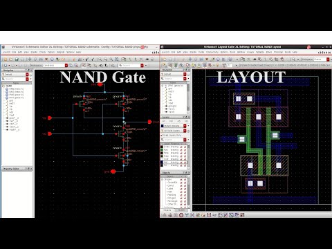
Cadence Virtuoso:: Layout of NAND Gate || Part-2. - YouTube

Lab

Lab 03 CMOS Inverter and NAND Gates with Cadence Schematic Composer

Cadence tutorial -CMOS NAND gate schematic, layout design and Physical